- 您现在的位置:买卖IC网 > Sheet目录2000 > IDT5V41064NLGI (IDT, Integrated Device Technology Inc)IC CLK GEN 1:1 16QFN
IDT5V41064
1 OUTPUT PCIE GEN1/2 SYNTHESIZER
IDT 1 OUTPUT PCIE GEN1/2 SYNTHESIZER
7
IDT5V41064
REV G 112111
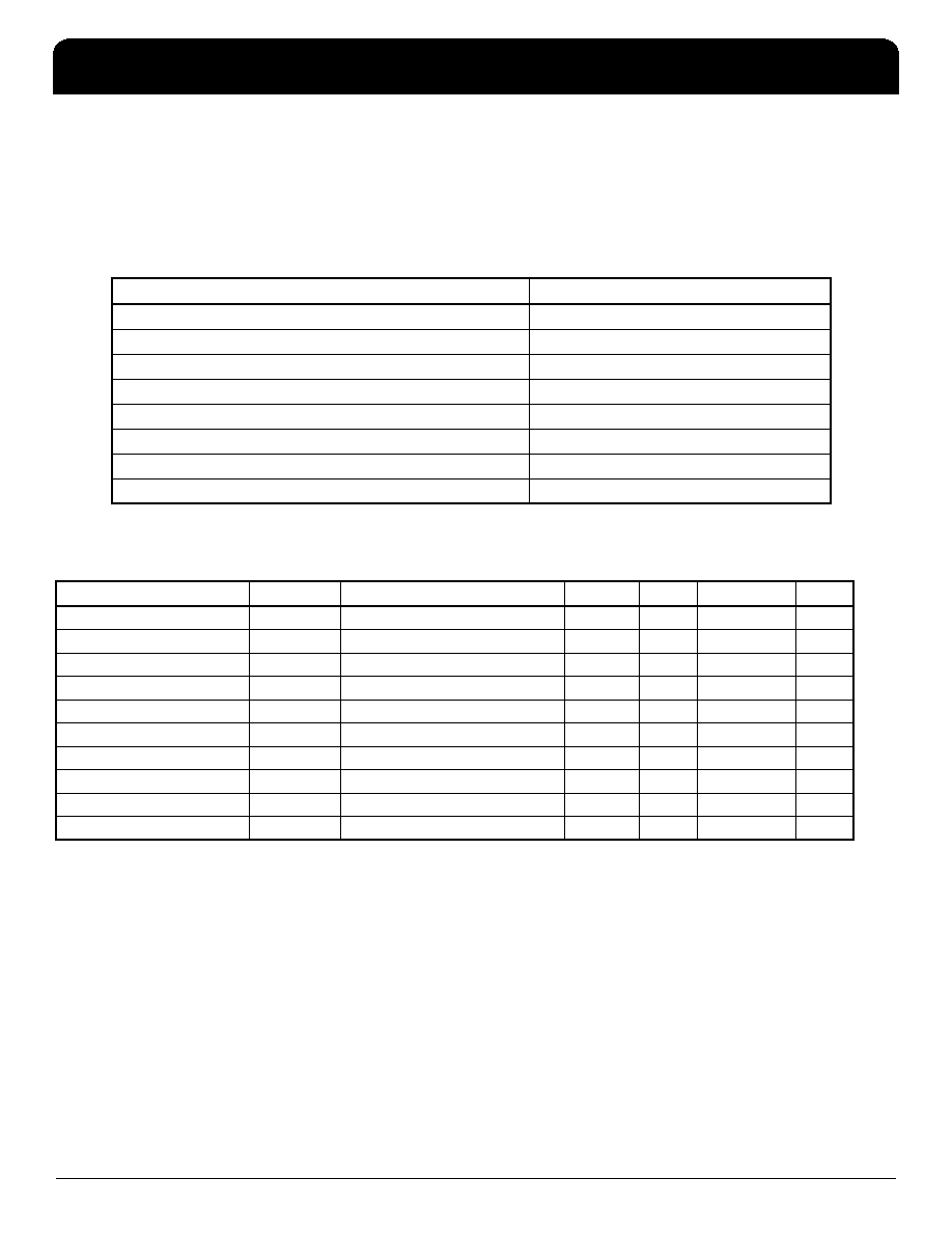
Absolute Maximum Ratings
Stresses above the ratings listed below can cause permanent damage to the IDT5V41064. These ratings are stress
ratings only. Functional operation of the device at these or any other conditions above those indicated in the
operational sections of the specifications is not implied. Exposure to absolute maximum rating conditions for
extended periods can affect product reliability. Electrical parameters are guaranteed only over the recommended
operating temperature range.
DC Electrical Characteristics
Unless stated otherwise, VDD = 3.3 V ±5%, Ambient Temperature -40 to +85
° C
1 Single edge is monotonic when transitioning through region.
2 Inputs with pull-ups/-downs are not included.
Item
Rating
Supply Voltage, VDD, VDDA
5.5 V
All Inputs and Outputs
-0.5 V to VDD+0.5 V
Ambient Operating Temperature (commercial)
0 to +70
° C
Ambient Operating Temperature (industrial)
-40 to +85
° C
Storage Temperature
-65 to +150
° C
Junction Temperature
125
° C
Soldering Temperature
260
° C
ESD Protection (Input)
2000 V min. (HBM)
Parameter
Symbol
Conditions
Min.
Typ.
Max.
Units
Supply Voltage
V
3.135
3.465
Input High Voltage1
VIH
2.2
VDD +0.3
V
Input Low Voltage1
VIL
VSS-0.3
0.8
V
Input Leakage Current2
IIL
0 < Vin < VDD
-5
5
μA
Operating Supply Current
IDD
2 pF load
70
mA
Input Capacitance
CIN
Input pin capacitance
7
pF
Output Capacitance
COUT
Output pin capacitance
6
pF
Pin Inductance
LPIN
5nH
Output Resistance
Rout
CLK outputs
3.0
k
Ω
Pull-up Resistor
RPUP
SS1
100
k
Ω
发布紧急采购,3分钟左右您将得到回复。
相关PDF资料
IDT5V41066PGG
IC CLK GEN SPRED SPECTRM 20TSSOP
IDT5V49EE901NLGI8
IC PLL CLK GEN 200MHZ 32VFQFN
IDT5V49EE902NLGI
IC CLOCK GEN PLL 500MHZ 32VFQFPN
IDT5V49EE904NLGI8
IC PLL CLK GEN 200MHZ 32VFQFN
IDT821024PPG
IC PCM CODEC QUAD NONPROG 44TQFP
IDT821034DNG
IC PCM CODEC QUAD MPI 52-PQFP
IDT821054PQF
IC PCM CODEC QUAD MPI 64-PQFP
IDT82V3001APVG8
IC PLL WAN W/SGL REF INP 56-SSOP
相关代理商/技术参数
IDT5V41064NLGI8
制造商:Integrated Device Technology Inc 功能描述:IC CLOCK BUFFER ZD 2.5V 16QFN
IDT5V41065NLG
制造商:Integrated Device Technology Inc 功能描述:IC CLK GEN SPRED SPECTRM 16NLG
IDT5V41065NLG8
制造商:Integrated Device Technology Inc 功能描述:IC CLK GEN SPRED SPECTRM 16NLG
IDT5V41065NLGI
制造商:Integrated Device Technology Inc 功能描述:IC CLK GEN SPRED SPECTRM 16NLG
IDT5V41065PGG
功能描述:IC CLK GEN SPRED SPECTRM 16TSSOP RoHS:是 类别:集成电路 (IC) >> 时钟/计时 - 专用 系列:PCI Express® (PCIe) 标准包装:1,500 系列:- 类型:时钟缓冲器/驱动器 PLL:是 主要目的:- 输入:- 输出:- 电路数:- 比率 - 输入:输出:- 差分 - 输入:输出:- 频率 - 最大:- 电源电压:3.3V 工作温度:0°C ~ 70°C 安装类型:表面贴装 封装/外壳:28-SSOP(0.209",5.30mm 宽) 供应商设备封装:28-SSOP 包装:带卷 (TR) 其它名称:93786AFT
IDT5V41065PGG8
制造商:Integrated Device Technology Inc 功能描述:IC CLK GEN SPRED SPECTRM 16TSSOP
IDT5V41065PGGI
功能描述:IC CLOCK SYNTHESIZER 16TSSOP RoHS:是 类别:集成电路 (IC) >> 时钟/计时 - 专用 系列:- 标准包装:1 系列:- 类型:时钟/频率发生器,多路复用器 PLL:是 主要目的:存储器,RDRAM 输入:晶体 输出:LVCMOS 电路数:1 比率 - 输入:输出:1:2 差分 - 输入:输出:无/是 频率 - 最大:400MHz 电源电压:3 V ~ 3.6 V 工作温度:0°C ~ 85°C 安装类型:表面贴装 封装/外壳:16-TSSOP(0.173",4.40mm 宽) 供应商设备封装:16-TSSOP 包装:Digi-Reel® 其它名称:296-6719-6
IDT5V41065PGGI8
制造商:Integrated Device Technology Inc 功能描述:IC CLK GEN SPRED SPECTRM 16TSSOP